Pulsed Laser Interference Lithography
Upon illumination of a surface or a thin film with an interference pattern of a pulsed laser a permanent structure might be induced. Although this process can be observed on a variety of surfaces the physical mechanisms behind are not well understood. We study therefore the ongoing processes on different surfaces by time-resolved methods as well as by characterization of the surface by scanning electron microscopy and atomic force microscopy. As the technique allows the periodic structuring of surfaces on sizes of several mm2 with periods ranging from 100 micron down to 150nm with a single laser pulse, it is a very flexible and fast approach for surface structuring. There-fore we study possible applications of this method as well.
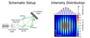
Experimental setup
We use single nanosecond pulses of an injection seeded Nd:YAG laser at the wavelengths 1064nm, 532nm or 266nm to generate an interference pattern. For that purpose the beam is split into several beams by beam splitters. These individual beams are then directed towards the surface to be structured by the help of mirrors. There an interference pattern is formed, which depends on the number of beams, their wavelength, polarization and the angles between the beams.
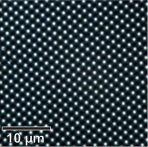
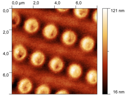
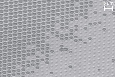
Surface appearance after illumination at low intensities
Above a material dependent energy threshold a permanent surface structure can be observed. We show here some examples of patterned surfaces.
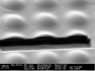
Especially on thin films structures appear which are on a first look difficult to explain. The feature height of the metallic hillocks can be larger than the film thickness.
A cut through the structure by a focussed ion beam clarifies this observation. The hillocks formed are hollow with an increased film thickness in the middle. We propose therefore that the metallic film is detaching from the surface in the liquid state
Surface appearance after illumination at high intensities
At high intensities the formed membranes are not stable anymore. Thus a dewetting process set in. As a consequence the metallic liquid is withdrawn from the illuminated areas. Thus a conducting transparent network can formed.
Structuring of Thin Magnetic Films
Here, we used the principle of direct laser interference patterning to produce one- and two-dimensional patterns on various magnetic thin films.
Studying [Co/Pd] multilayer thin films, we showed that one-dimensional magnetic domains with periods down to 600 nm and a width of 120 nm can be induced.
For more details see:
M. Stärk et al. 2015 Nanotechnology 26 205302 doi:10.1088/0957-4484/26/20/205302
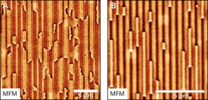
MFM images of a [Co/Pd] thin film illuminated with a 1 µm (A) and 650 nm (B) interference pattern. A transition from domain walls oriented in various direction towards a very well ordered state is shown.