
Optical Nearfields/Plasmonics
An electromagnetic field which interacts with metallic materials might be modified in a way that locally confined fields exist in the surrounding of the metallic structure. We study such optical nearfields by an unconventional method: the enhanced field is used for local ablation of the silicon substrate below the metallic structure by a femtosecond laser pulse. The ablation region, which reflects the local field can then be imaged with an atomic force microscope (AFM).
Experimental setup:
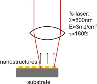
A fs-laser pulse is mildly focussed onto the substrate with the metallic structures. After a single shot the surface is analyzed by AFM or electron microscopy.
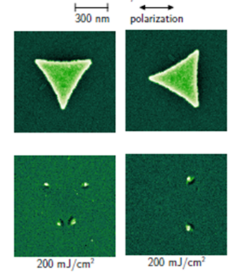
Electron microscopy of ablated material which show how the nearfield pattern depends on the polarization of the material.
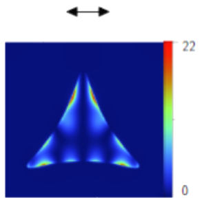
A comparison the FTDT-simulation shows the expected nearfield distribution.